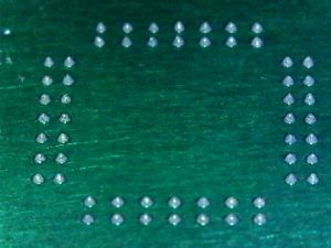
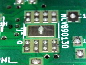
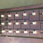
The Keska internally developed Micro Dot solder process is a great option for individual (R&D) PCB assembly. Using Micro Dot soldering, the traditional costs for the stencil and the printer set-up time are eliminated. The equipment is programmed using standard Gerber Paste files, thereby eliminating all programing time for the process.
The Micro Dot soldering process is also environmentally friendly. There is no solder waste resulting from this solder paste application process. There are also no solvents required to clean-up paste residue. The solder remains in a sealed print head or precisely placed on the circuit board, which is unique to prototype circuit board assembly manufacturing.
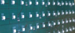
This process is ideally suited for LED PCB assembly, high chip count PCB's, and many other builds where hand soldering or stencil printing is being considered for R&D (1-5pcs) builds. Minimum chip size is a limited to 0402, and a minimum pad dimension of 0.35mm is required.
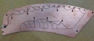
Keska LLC has developed process' specifically for large scale, quick turn surface mount LED circuit board assembly. Using in-house CNC manufacturing technology Keska LLC can quickly build low cost LED circuit boards with sizes up to 16" x 20". Starting with bare copper clad board keeps our direct materials cost extremely low allowing for very competitive pricing. Using this in-house developed method, we are capable of supporting 1-Day turn around on LED circuit board assemblies!

